High-NA EUV lithography challenges – the imec perspective
In the course of 2025, the introduction of the first high-NA (numerical aperture) extreme ultraviolet (EUV) lithography equipment in high-volume manufacturing environments is foreseen.
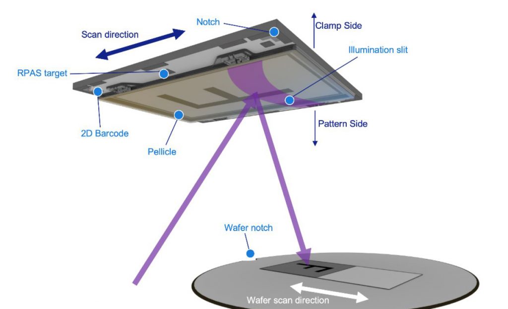
These next-generation lithography systems will be key to advance Moore’s Law towards the logic 2-nm technology generation and beyond. In this Mikroniek article, imec scientists and engineers involved in preparing this major next step in semiconductor lithography (driven by equipment maker ASML) discuss challenges and opportunities. They highlight recent insights and progress obtained in developing the patterning processes, metrology and photomasks needed for enabling the high-NA EUV lithography infrastructure. (Image courtesy of imec)